EQUIPMENT NETWORK
PCB production and testing equipment.
Representative resources available through selected manufacturing partners for project-specific process and quality requirements.
PARTNER EQUIPMENT NETWORK
Production and testing resources for demanding PCB projects.
Review representative production and inspection resources by category. Exact equipment, capability, calibration and reporting scope are confirmed with the selected manufacturing partner before order placement.
PRODUCTION EQUIPMENT
Production Equipment
Representative imaging, drilling, routing, surface-treatment and lamination resources available through selected PCB manufacturing partners.
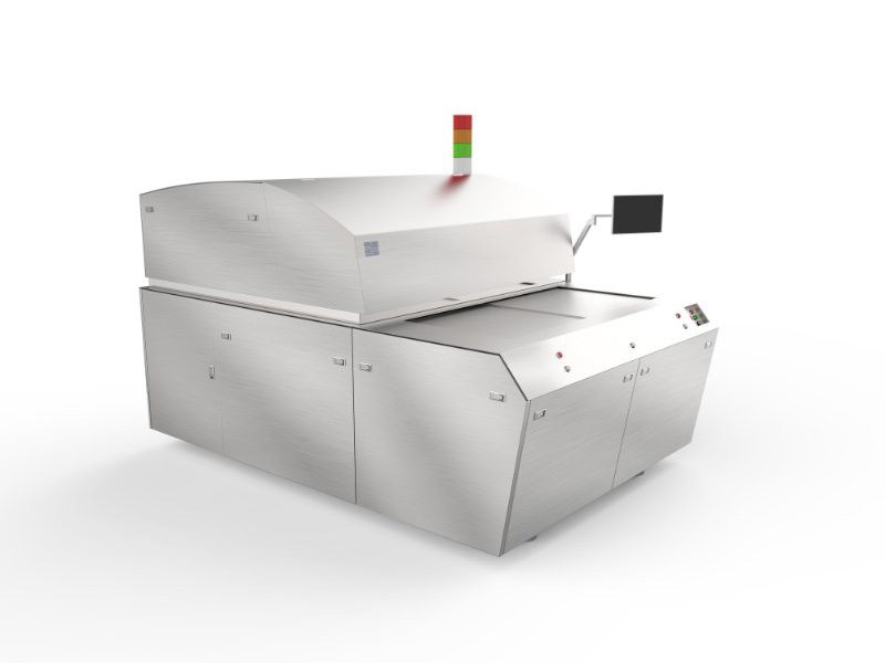
Laser Direct Imaging
Direct imaging supports accurate circuit registration and fine-line production without conventional film tooling.
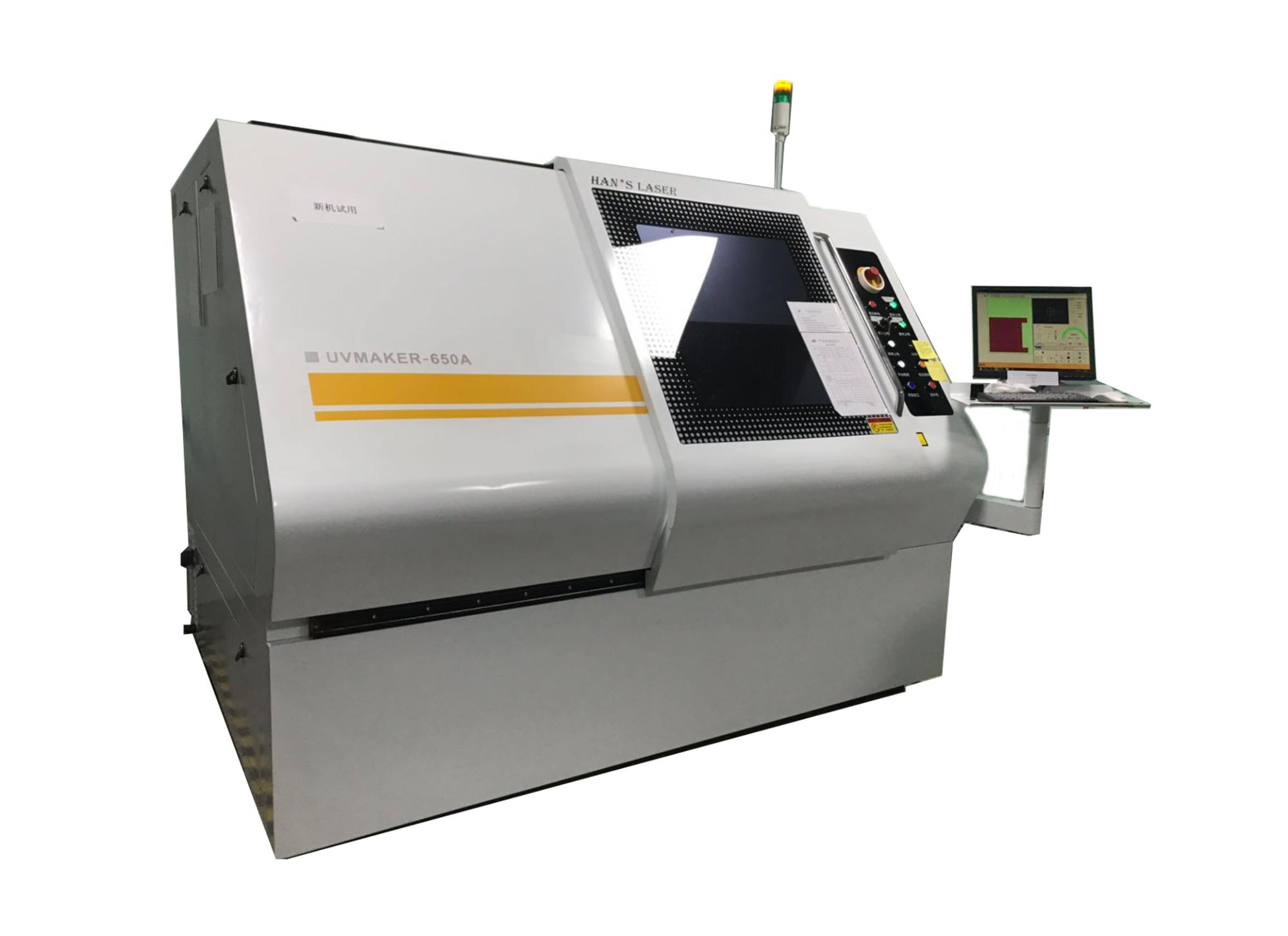
UV Laser Cutting Machine
UV laser processing supports precise profiling of thin, flexible and high-density circuit materials.
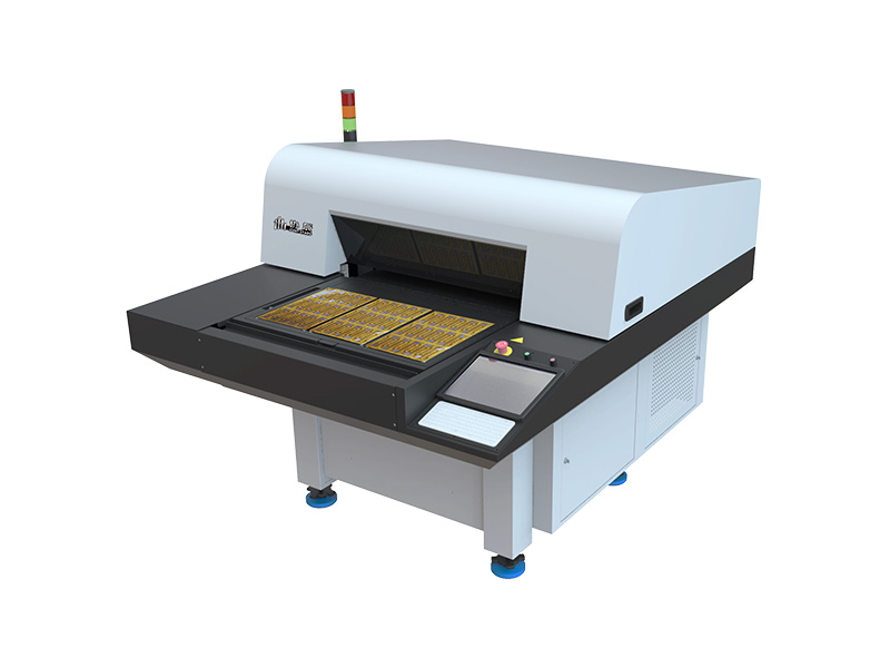
Legend Inkjet Printer
Digital legend printing improves marking consistency and supports flexible small-batch production.
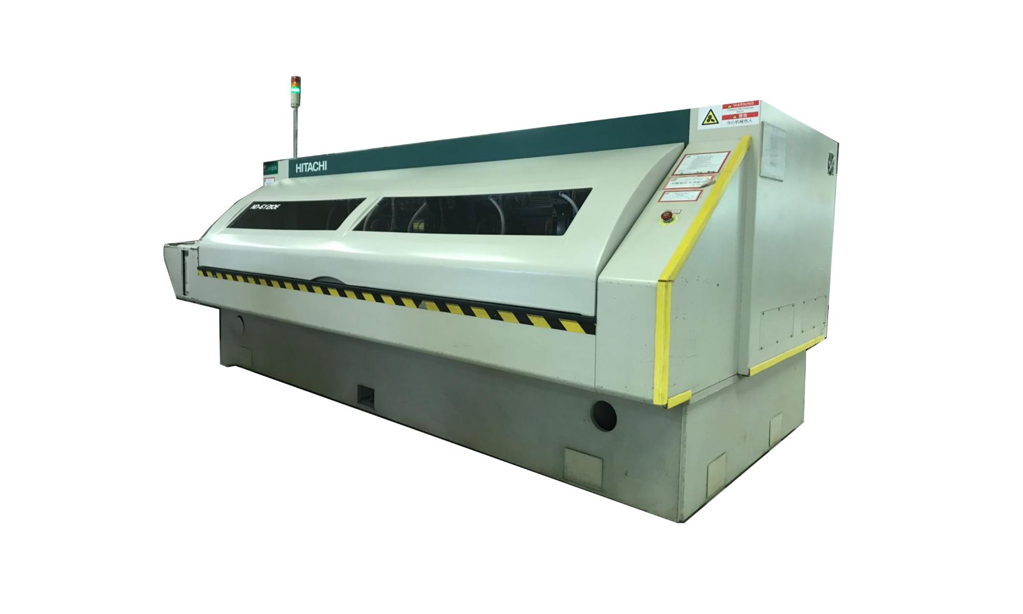
Hitachi Drilling Machine
High-speed CNC drilling supports controlled hole position, diameter and multilayer registration.
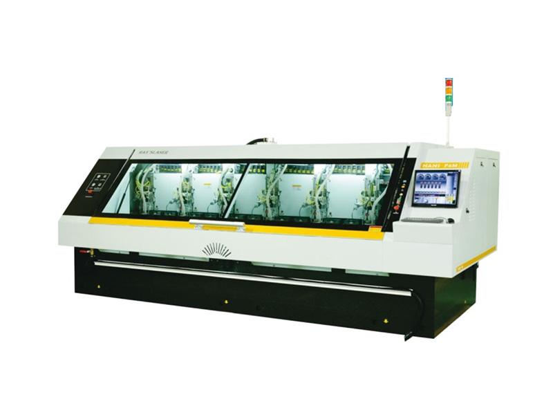
Automatic CNC Routing Machine
Automated routing provides repeatable board outlines, slots and panel separation profiles.
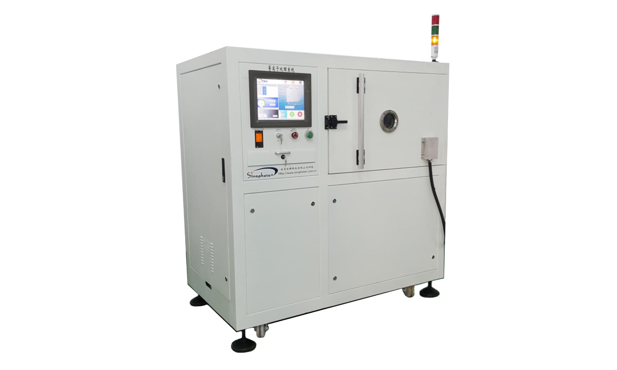
RF / HF PCB Plasma System
Plasma treatment supports reliable hole-wall preparation for demanding RF and high-frequency laminates.
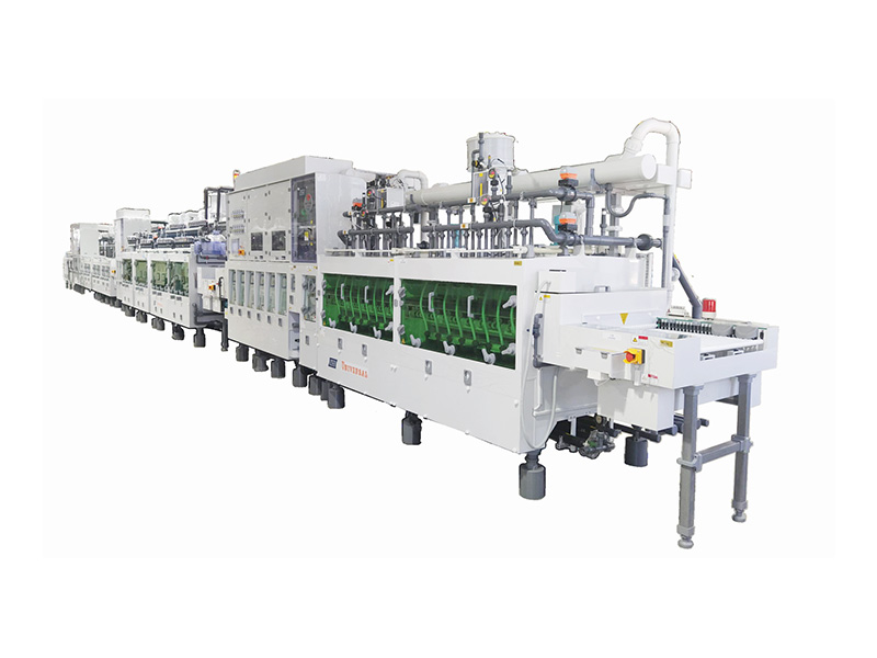
Automatic Horizontal Line
Horizontal wet-process automation supports stable chemistry control and repeatable surface treatment.
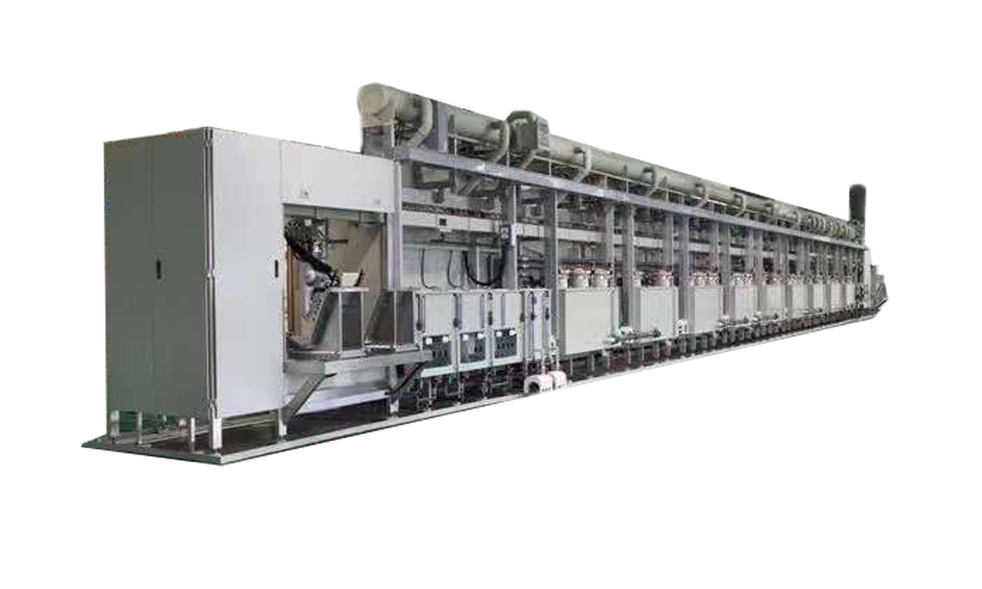
VCP Line
Vertical continuous plating supports uniform copper deposition across panel surfaces and plated holes.
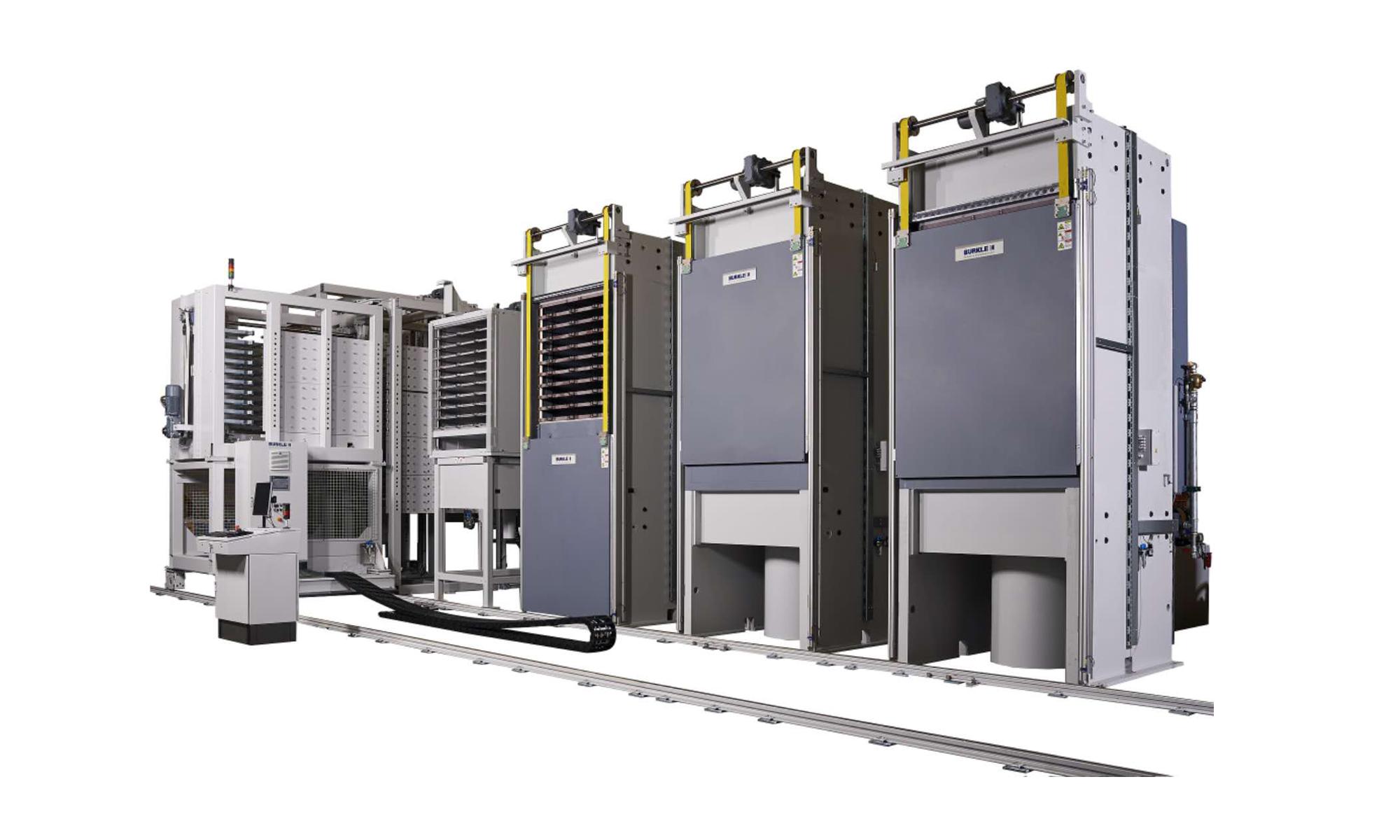
Multilayer Board Pressing Machine
Controlled heat and pressure cycles support consistent multilayer lamination and dimensional stability.
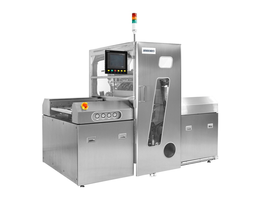
Automatic Dry Film Line
Automated cleaning and lamination improve dry-film adhesion and production consistency.
TESTING EQUIPMENT
Testing Equipment
Representative dimensional, material, electrical and thermal verification resources available for project-specific quality plans.
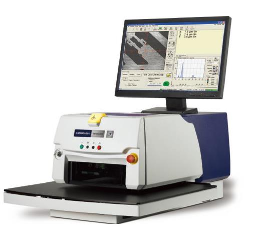
Gold Thickness Tester
X-ray fluorescence measurement supports verification of plated thickness and surface-finish composition.
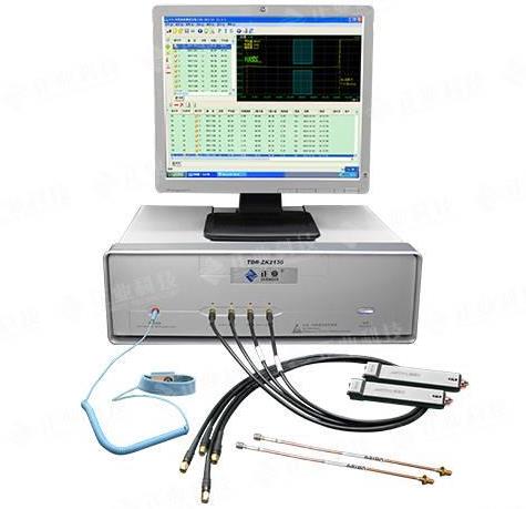
Impedance Tester
Controlled-impedance coupons can be measured and documented against the confirmed stack-up requirement.
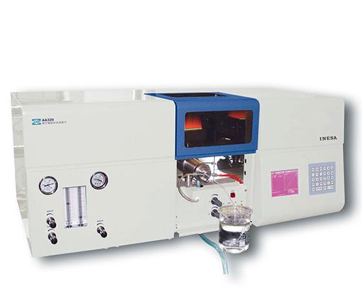
Atomic Absorption Spectrophotometer
Analytical measurement supports process-chemistry control and material-composition verification.
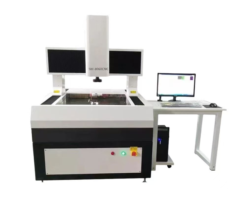
2D Measurement System
Optical dimensional inspection supports checks of profiles, hole positions and critical board geometry.
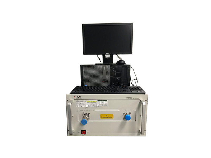
Intermodulation Tester
Passive-intermodulation evaluation is available for relevant high-frequency and RF board applications.
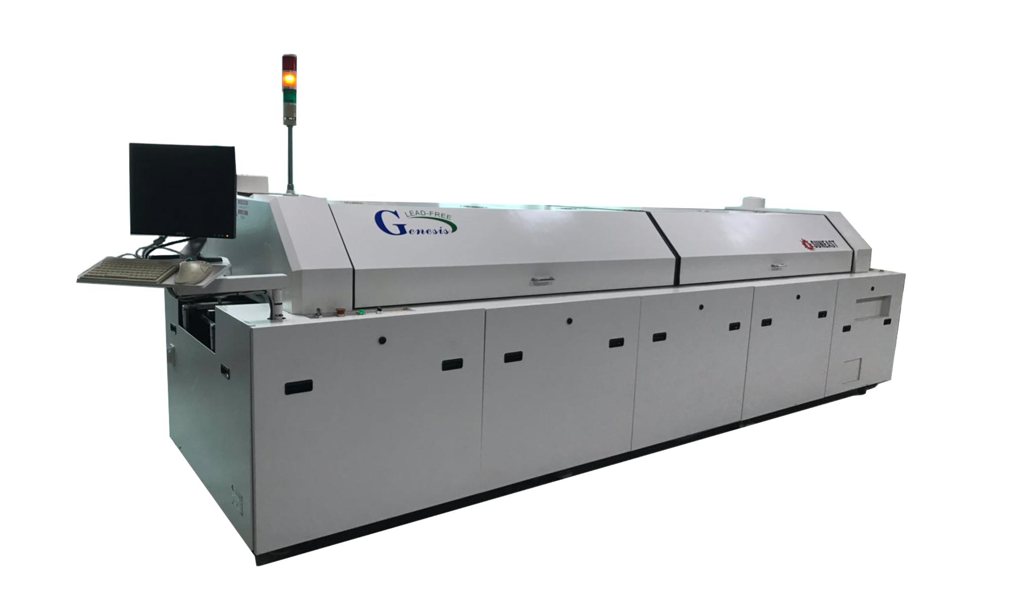
IR Furnace
Controlled thermal exposure supports process verification and heat-resistance evaluation when specified.
PROJECT-SPECIFIC CONFIRMATION
Match the process and inspection plan to your PCB specification.
Equipment availability, capability, calibration scope, inspection frequency and report format are confirmed with the selected manufacturing partner for each order. Images show representative partner resources and do not imply asset ownership by JULY SEVEN.